Elephantech wants to create circuit boards that are kinder to the environment • ZebethMedia
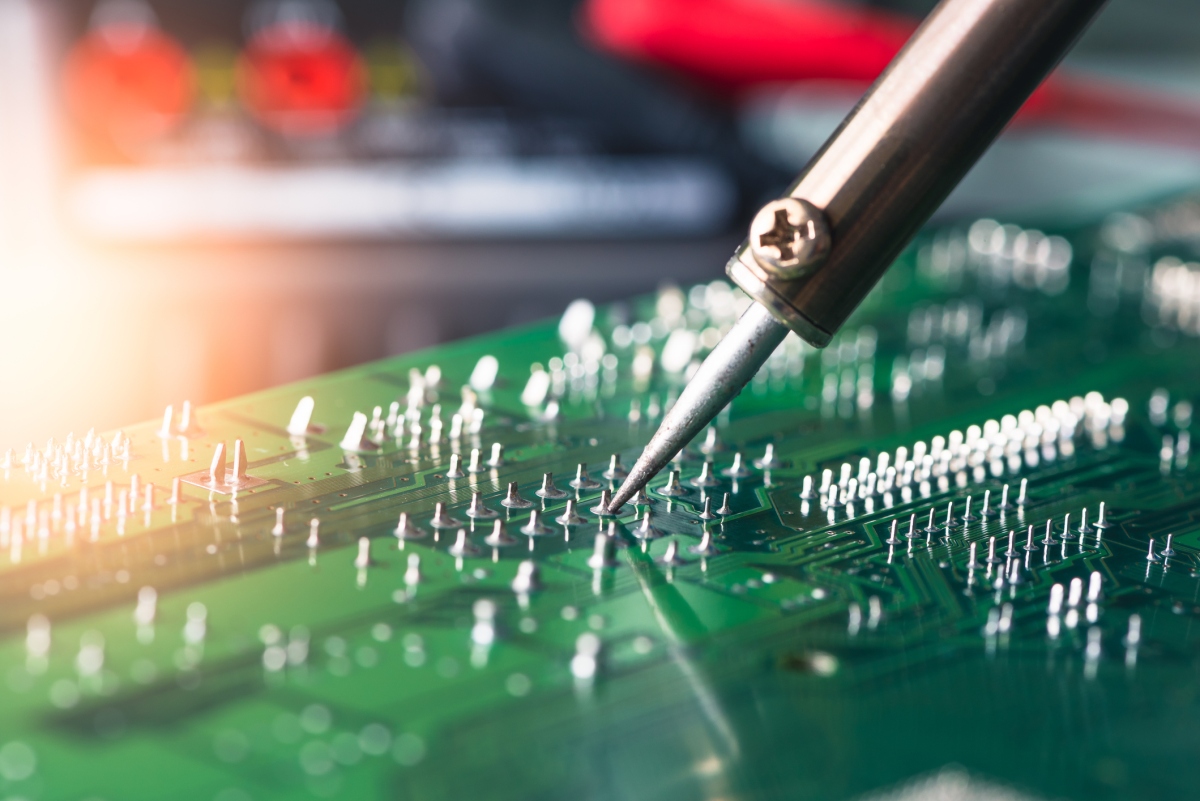
Printed circuit boards (PCB), which perform essential functions in electronic devices, including displays and sensors, need a lot of energy to create. Moreover, traditional PCB manufacturing processes generate large amounts of liquid waste and high carbon emissions. Still, there are more environmentally friendly ways of producing PCBs, including additive manufacturing processes that use inkjet and laser printing, while fully biodegradable PCBs are also on the horizon. To get its slice of $90 billion PCB manufacturing pie, Tokyo-based startup Elephantech has developed an eco-friendly PCB called P-Flex, using inkjet printing-based electronic circuit manufacturing technology which it says reduces carbon emissions by 77% and water consumption by 95% compared to conventional processes. The main change Elephantech ushers in to the PCB process is that while electronic circuits are typically made through so-called “subtractive” manufacturing which involves layering an entire surface with metal before dissolving the areas that aren’t necessary, with Elephantech’s “pure additive” process, it only puts metals in place where they are needed to begin with. Nothing is subsequently removed (i.e. wasted). The company also says that its nanoparticle inkjet technology helps cut costs by 32%, through removing a number of procedures from the manufacturing process. To meet its mission “to create a sustainable world through resource-and energy-efficient manufacturing technologies,” Elephantech has secured 2.15 billion yen (~$15 million) in funding, at a 12.3 billion yen ($88 million) valuation, a company spokesperson told ZebethMedia. The new capital, which brings its total raised to approximately 7 billion yen ($50 million) since its inception in 2014, will help the startup scale its business from R&D and its current production volume, which is focused on its domestic market, to target customers globally. Regular circuit Elephantech started the mass production of its PCBs two years ago in its Nagoya facility, and while it is currently focused on single-sided flexible substrates, it plans to produce multi-layered and rigid PCBs, which constitute different layers, including a copper layer, substrate layer and silkscreen layer. The company said that its inkjet printing technology can also be used in other sectors such as healthcare, optics, and textiles. In August, the startup announced a dye removal technology called neochromato, co-developed with Japanese textile chemical company Nicca Chemical. The neochromato process supports removing print from polyester fabrics without using water, and putting new print on the textiles to reuse the material with a different design before recycling to reduce apparel waste. The outfit said the process could reduce about 48% of CO2 emissions when clothes are recycled with a different pattern compared to chemical recycling, which reduces about 20% of the carbon emissions. A number of fledgling startups are working to address and optimize different aspects of the PCB design process, including a company called Celus, which recently raised $25.6 million for a platform that automates circuit board design. Then there’s Luminovo, which secured $11 million to reduce waste in PCB manufacturing by bringing together the entire material and production costing process. So it’s clear that there is a growing impetus to optimize and improve on a technology that powers just about every electronic contraption there is, from smartphones to microwave ovens. Combined with growing environmental concerns and the role that electronics plays in that, Elephantech is perhaps in a strong position to gain traction in global markets, and its latest cash injection will go some way toward helping. Elephantech’s funding round included investments from Anri V Investment, Shin-Etsu Chemical, Nose, Shizuoka Capital, Eiwa Corporation, Nanobank, Mitsubishi Gas Chemical, Kenbishi Sake Brewing, D&I Investment, Epson, Sumimoto, East Ventures and Beyond Next Ventures.